【光谱实验室:陈中博士 撰文】
【仪器设备:快速成像显微拉曼光谱仪WITec R300】
【地点:4号楼220室 光谱实验室】
目前最新型拉曼光谱仪的应用早已不仅限于拉曼光谱的谱学分析,拉曼共聚焦成像由于其不需要进行额外标记、相对于荧光共聚焦、减少了繁琐的标记物的设计和选择,越来越受到研究人员的重视。理化平台光谱实验室的“快速成像显微拉曼光谱仪”基于光纤共聚焦设计和高灵敏度光谱仪,实现光学衍射极限空间分辨(横向≤300 nm,纵向≤900 nm),在拉曼成像方面能充分保证共聚焦的优异性能。当样品拉曼信号很弱(单点积分时间长)或者扫描范围非常大(面积大,扫描点数多)时,高分辨率拉曼成像往往需要非常长的成像时间,长时间成像过程中的各点扫描都会受到环境噪音与振动的影响,即使优异的共聚焦系统也难以保证超长时间每一点的焦平面都保持稳定不脱焦。为了解决这个问题,本仪器在硬件上配置了TrueSurface (TS)实时聚焦模块,能确保拉曼成像时根据表面的形貌进行实时快速聚焦。这种方式将使用了先进的光学轮廓仪集成在仪器内,以专门的独立光路实时反馈表面形貌,并根据形貌即时调整镜头高度、完成同步成像。 所以,TS功能在扫描范围内实现了实时的采集表面轮廓和拉曼成像,不仅能解决平整样品长时间成像时周围环境造成的脱焦效应,也能实现粗糙表面或倾斜表面的样品成像。

图1 光路系统的聚焦和脱焦。
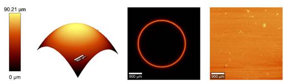
图2 Si透镜成像。左:透镜的表面形貌。中间:普通的共焦拉曼显微镜只能聚焦一个深度。右图:与中间的图像相同,但TrueSurface激活后,Si信号从各个深度都是恒定的,因为样本表面实时聚焦。
首先,我们选用Si透镜的成像例子来描述其成像功能。Si的拉曼峰在520.7cm-1, 拉曼信号非常强,但当Si的表面加工成表面弧形的时候(左图),即使很强的拉曼信号用普通的共聚焦拉曼成像只能得到一个强拉曼信号环(中间),无法得到硅表面的全部信号,因为只有环形区域处于聚焦状态,其他区域都是脱焦的。右边的图像显示了TS激活后测量的相同区域,TS保证了实时调节显微镜与样品的距离,保证在样品的每个点的成像都是聚焦的,从而获得了整个区域上的高分辨率拉曼成像。
基于上述的原理,我们再选用一个弱信号且表面粗糙的样品Y3Al5O12 (YAG,理化平台性能测试实验室聂颖博士提供,https://iscps.westlake.edu.cn/info/1148/1073.htm),此材料是激光器材料,非常耐激光照射,并且切割机的局限,样品表面起伏度在µm级,如图3a和3b所示黑色区域和白色区域并不在同一个焦平面上。同时,因为此样品生长的时候,其物相并不是完全均匀的,如图3c所示,在红色标记和蓝色标记的地方各自先聚焦清晰后再进行拉曼单点扫描,发现有两类形貌有着完全不同的拉曼信号,这些特点使它作为一个DEMO样品能充分发挥TS的强大功能。

图3 YAG样品上的两种区域(红色十字和蓝色十字)呈现出完全不同的拉曼位移
我们对图3上的红框所包含样品作为拉曼成像,扫描范围为90 µm×90 µm,像素为270×270像素,扫描拉曼空间分辨率大约为300 nm。由于YAG的拉曼信号弱,我们将激光功率调到最高功率50mW,每个像素点积分时间为1秒,成像总耗时为(270×270/3600)=20.25小时,是一个超长时间的拉曼成像。我们在同一区域,其他扫描条件保持一致,用普通拉曼成像和TS开启的拉曼成像各完成一次。

图4. 普通拉曼成像和开启TS后拉曼成像 (a).光学图上选取拉曼成像的区域;(b) TS获得的样品表面高度轮廓图,结果表明样品高度差可达20 mm;(c) 782 cm-1的普通拉曼成像;(d) 782 cm-1的TS拉曼成像;(e) 552 cm-1的普通拉曼成像;(f) 552 cm-1的TS拉曼成像
根据图3的拉曼位移,我们首先确定两个特征峰,其中光学图像上看到黑灰的区载含有782 cm-1峰位,而突出的白色区域在552 cm-1具有较强的特征信号。图4b是TS功能开启后,TS光路对样品表面进行实时聚焦后得到的轮廓图,结果表明样品高度差达20 mm。图4c是782 cm-1下的普通的拉曼成像,发现所成的像非常模糊,这是由样品的粗糙表面导致脱焦所致。而同样的条件下,开启TS功能后,所成的像非常清晰,即使成像时间达到了20小时,也丝毫没有发现脱焦现象,图4的e和f中552 cm-1的成像也同样证明了TS功能的强大。所以TS功能不仅能根据样品表面的粗糙度实时调整高度,同时自身也非常稳定,超长时间成像都不会产生脱焦现象。
本专题用实例介绍了“快速成像显微拉曼光谱仪”的TS功能对拉曼成像的作用,根据实验的结果,如果待测样品本身粗糙是需要开启TS功能来校正样品表面的起伏;如果待测样品非常平整,拉曼信号非常强,成像时间会非常快,环境因素影响少,不必开启TS。但是平整的弱信号样品需要的成像时间很少,为了避免环境噪声的干扰,建议此时开启TS功能。
理化平台的“快速成像显微拉曼光谱仪”除了具有TS功能外,还具有低波数测试、光电流成像、低温成像等一系列强大的功能,在以后的技术专题中我们会逐一进行介绍,敬请关注。
Fast-Mapping Micro-Raman Spectrometer——Principle and Application of TrueSurface Module
Nowadays, the applications of Raman spectroscopy has long been not limited to the spectral analysis of Raman, and the free-label Raman confocal mapping and imaging has attracted incredible attentions because it doesn’t require the design and selection of markers that is necessity by the means of fluorescence confocal imaging. Our Spectroscopy Laboratory at ISCPS provides the “Fast-Mapping Micro-Raman Spectrometer” equips with the optical fiber confocal design and high sensitivity spectrometer, which can reach to the optical diffraction limit spatial resolution (transverse ≤ 300 nm, longitudinal ≤ 900 nm), and also fully guarantee the excellent performance of confocal in Raman mapping and imaging. In generally, when the Raman signal of sample is very weak (require long integration time), or scanning range is very large (require many scanning points), getting a high-resolution Raman mapping is always a time-consuming process. In that case, the point-by-point scanning will be influenced by ambient noise or mechanical oscillation sooner or later. Even an excellent confocal system is difficult to guarantee full-time in-focal in the process of mapping. To solve this problem, our Raman instrument is equipped with TrueSurface (TS) real-time focusing module, which is a surface morphology dependent real-time focusing system. In this way, an advanced optical profilometer is integrated into the instrument, in which a specialized optical path can provide real-time feedback on the surface topography and adjust the lens height based on the topography information to accomplish synchronous mapping. Therefore, the TS function achieves the real-time surface contour collection and Raman mapping within the scanning range, which can not only solve the defocusing effect caused by the surrounding environment, but also suitable for the Raman mapping of samples with rough or inclined surfaces.

FIG. 1 In focus and out of focus of optical path system.

FIG. 2 Si lens. Left: Topography. Middle: Only one depth level is in focus with the standard confocal Raman microscope. Right: The same image as in the middle, but with TrueSurface activated the Si signal is constant from all depths as the sample surface is always kept in focus.
First, the effect is demonstrated in FIG. 2 on a silicon lens. The image on the left shows the topography of the sample surface. Without TS, only one plane is in focus during a measurement, resulting in a ring of strong Raman signal (middle). The image on the right shows the same area measured with TS active, which allows the acquisition of a Raman map with a consistently strong signal.
To better describe the performance of TS, we dedicatedly choose a weak signal sample with rough surface Y3Al5O12 (YAG, provided by Physical Properties Characterization Lab, https://iscps.westlake.edu.cn/info/1148/1073.htm), this material is one kind of laser material that very resistant to the laser irradiation. Due to the limitations of cutting machine, the cut surface is not completely smooth and its roughness is at micrometer level, as shown in FIG 3a and 3b, the black region and the white region are not on the same focal plane. Also, the black region (red cross) and the while region (blue cross) exhibit completely different Raman shift excited by strong laser, which indicate the phase of YAG is not completely uniform. So, the characteristics of rough surface, weak signal and nonuniform make it as a good DEMO sample that fully give play to the powerful performance of TS module.

FIG 3. The two regions (Red Cross and blue cross) on the YAG sample exhibit completely different Raman shift
Furthermore, Raman mapping was used to image the samples area showed in the red square box in FIG 3, with a scanning range of 90 μm ×90 μm and pixels of 270 × 270, leading to a scanning Raman spatial resolution of about 300 nm. Due to the weak Raman signal of YAG, we increased the laser power up to the maximum power of 50 mW. The integration time set as 1s/pixel, and the total collecting time is (270 × 270 / 3600) = 20.25 hours, which is a time-consuming Raman mapping. Here, the standard Raman mapping and TS activated Raman mapping were performed independently at the same region.

FIG 4. Standard Raman mapping and TS activated Raman mapping. (a). the selected mapping area in bright photo. (b). Surface profile of sample acquired by TS. (c) standard Raman mapping with 782 cm-1. (d) TS activated Raman mapping with 782 cm-1. (e) standard Raman mapping with 552 cm-1. (f) TS activated Raman mapping with 552 cm-1.
According to the Raman shift in FIG. 3, we first selected two representative peaks from YAG sample, where the black gray area in the optical image shows characteristic peak at 782 cm-1, while the prominent white area has a strong feature signal at 552 cm-1. FIG 4b show the surface profile of sample by the real-time focusing guided by TS module. FIG 4c is a standard Raman mapping collected by 782 cm-1 signal. It is found that the resulting image is very fuzzy, which is caused by the defocusing of the rough surface of the sample or ambient environment. Once the TS function is activated, the acquired image become very clear (FIG 4d). The results show that even if the mapping time reaches 20 hours, there is no defocusing phenomenon happen. The imaging of FIG 4e and FIG 4f (552 cm-1 signal) also proves the powerful function of TS. Therefore, the TS function can not only adjust the height in real time according to the roughness of the sample surface, but also guarantee the focal plane stability during the ultra-long-time data collecting.
This article introduces the effect of TS module of "Fast-Mapping Micro-Raman Spectrometer" on Raman mapping and imaging using a representative sample. Summarized from the experimental results, if the sample surface is rough, it is necessary to turn on TS module to correct the fluctuation of the sample surface. If the sample surface is very flat and its Raman signal is very strong, the scanning time will be very fast, the impact of environmental factors is neglect, it is not necessary to turn on TS. For the flat sample with weak Raman signal, it needs to increase the integration time to enhance Signal/Noise Ratio, in order to avoid the interference of environmental noise, it is recommended to activate TS function at this time.
In addition to TS module, the "Fast-Mapping Micro-Raman Spectrometer” also provides a series of powerful functions such as low wavenumber Raman spectroscopy test, photocurrent imaging, and low temperature imaging, which will be introduced one by one in the following technical topics. Welcome to the Spectroscopy Laboratory of ISCPS to discuss and use "Fast-Mapping Micro-Raman Spectrometer".