【光谱实验室:陈中博士 撰文】
【仪器设备:紫外可见(近红外)光谱仪】
【地点:4号楼220室 光谱实验室】
对于金属导体、绝缘体和半导体来说,因其导电性不同,所以其能带结构也不相同。金属的能带是重叠,或是半填满,所以在一个能带内总是既有电子又有空能态,电子在电场作用下便能自由运动,从而导致很高的导电性。绝缘体与半导体的导电性在本质上是相同的,差别仅在于禁带宽度(带隙)不同,例如Si为1.1 eV,而金刚石为5.0 eV。绝缘体在足够高的温度下,也可以认为是半导体。因为绝缘体与半导体的能带结构具有很大的共同点——存在禁带,只是宽度有所不同而已。
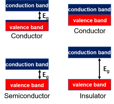
图1 导体、半导体和绝缘体的能带图
禁带宽度是半导体材料中一个衡量导电性能好坏的重要参量,它表示晶体中的(a)公有化电子所不能具有的能量范围;(b)价键束缚的强弱;(c)电子与空穴的势能差。在实际科研和应用中,对禁带宽度的测量是研究半导体材料性质的基本手段,禁带宽度可以通过电导率法和光谱测试法测得。为了区别于用电导率法测得禁带宽度值,用光谱测试法测得的禁带宽度叫做光学带隙。本技术专题基于紫外可见近红外分光光度计,介绍最常用的用于禁带宽度计算的光谱法。
根据半导体的导带底与价带顶对应K空间中位置是否一致,其带隙可以分为直接带隙和间接带隙,当采用吸收光谱法计算带隙时,两种带隙的计算方法是不一样的,所以首先简单介绍一下两者的区别。如图2所示,具有禁带宽度的材料,直接带隙对应的过程是:一个电子在K空间从价带顶激发到导带底并不需要声子的参与(也就是不会被晶体散射),因为导带底与价带顶在K空间的位置一致。而间接带隙对应的过程则需要声子参与,也就是说电子会被晶体散射,从而放出声子。而电子一开始是没有动量的,所以必须引入声子,因为动量方向必须满足动量守恒。
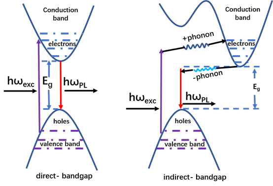
图2 直接带隙和间接带隙的能带图
禁带宽度的计算方法1,截线法:禁带宽度Eg的单位一般用eV表示,截线法是一种简易的求取半导体禁带宽度的方法,其基本原理是认为半导体的带边波长(也叫吸收阈值,λg)决定于禁带宽度Eg,两者之间存在如下的数量关系:
Eg (eV) = hν = h/k × C/λ = [6.63×10⁻³⁴ J•s] / [1.6×10⁻¹⁹ J/eV] × [3×10¹⁷ nm/s ]/λ = 1240/λg (nm)

图3 截线法计算禁带宽度Eg
如图所示,在吸收光谱的曲线上,沿着曲线变化最大位置的点做切线,记录切线与 x 轴的交点位置为λg,然后用1240/λg计算禁带宽度Eg。
禁带宽度的计算方法2,Tauc plot法:上述截线法适用于透射光谱的直接带隙测试,适用范围较窄,Tauc plot主要是基于Tauc,Davis和Mott等人提出的公式:(αhν)1/n = B(hν-Eg) , 其中α为吸光系数,h为普朗克常数,ν为频率,B为常数,Eg为半导体禁带宽度,指数n与半导体类型直接相关,直接带隙n=1/2, 间接带隙n=2。
由上述公式可知,(αhν)1/n只与hν成线性关系,能用于估算Eg。
通过Tauc plot来求取Eg时,不论采用Abs还是α其实对Eg值是不影响的(只不过是系数B有差异而已),所以简单起见,可以直接用吸光度Abs值替代吸光系数α。
下面以In2O3样品为实例具体步骤如下:
将In2O3均匀涂在石英片上,以石英片作基线,测试样品的吸收光谱:

图4 Tauc plot吸收光谱法计算带隙
在Origin中的每一栏中的参数如图4所示进行函数计算,由于In2O3是一种n型宽带隙半导体,既有直接带隙,又有间接带隙,计算直接带隙时,n=1/2, 以(Ahν)2= hν-Eg作图;计算间接带隙时,n=2, 以(Ahν)1/2= hν-Eg作图,如图5所示, hν 值为 x 轴,分别以(Ahν)2,(Ahν)1/2值为 y 轴作图,反向延伸曲线切线与 x 轴相交,即可得半导体材料的光学直接带隙 Eg=3.68 eV, 间接带隙Eg=2.85 eV,与之前已发表的结果直接带隙 Eg=3.6 eV[1-2], 间接带隙Eg=2.6 eV[2]非常接近。
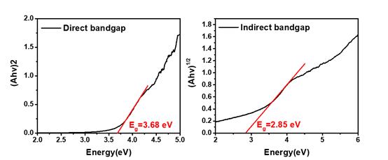
图5 In2O3的直接带隙和间接带隙计算
除了吸收光谱计算带隙,紫外可见漫反射光谱同样也可以用于直接带隙和间接带隙的计算,根据Kubelka-Munk公式, 源自这两位科学家Zeit. Für Tekn. Physik在1931年发表的反射理论:
(F(R)hν)1/n =K/S=(1-R)2/2R= B(hν-Eg)
其中K为吸收系数,S为反射系数,R为反射率(百分数形式),其中h为普朗克常量,ν是光的频率,Eg是一个与材料有关的物理量,即带隙能量值,n对于间接带隙型半导体是2,对于直接带隙型半导体是1/2,以(F(R)hν)1/n为纵坐标,hν为横坐标作图,对其中线性区段进行拟合,得到一个线性方程,它在x轴截距即是带隙能量的大小。
下面以Ga2O3样品为实例具体步骤如下:
先用BaSO4白板作反射光谱的基线,然后将样品均匀涂在BaSO4上,测试样品的反射率R。将所测的数据按图6的方法处理:
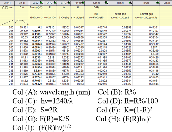
图6 Tauc plot反射光谱法计算带隙
在Origin中的每一栏中的参数如图6所示进行逐步计算,由于Ga2O3是一种直接带隙半导体,n=1/2, 以(F(R)hν)2= hν-Eg作图,如图7插图所示,hν 值为 x 轴,分别以 (F(R)hν)2值为 y 轴作图,反向延伸曲线切线与 x 轴相交,即可得半导体材料的光学直接带隙值 Eg。如果待测样品是间接带隙半导体,只需将y轴的值用(F(R)hν)1/2作图,反向延伸曲线切线与 x 轴相交,即可得半导体材料的光学间接带隙值Eg=4.72 eV,与前人的实验结果Eg=4.5~4.9 eV[3-4]相同。

图7 Ga2O3的直接带隙计算
本专题系统地介绍了如何用紫外可见近红外分光光度计测量半导体的禁带宽度,并用相应的实例证明了其计算结果的可靠性。欢迎大家来分子科学平台光谱实验室讨论和使用紫外可见(近红外)光谱仪。
UV-Vis-NIR spectrum for calculation of bandgap
Metal conductors, insulators and semiconductors have different energy band structure which leads to their different electrical conductivity. To be specific, the bands of metal are overlapped, or half-filled, therefore, the electrons can move freely under the electric field, resulting in high conductivity. The conductivity of an insulator and a semiconductor is essentially the same because of the bandgap, such as 1.1 eV for Si and 5 eV for diamond. In concept, Insulators can also be transformed into semiconductors at sufficiently high temperature since the bandgap of insulators will decrease with the increase of temperature, and semiconductors have a great deal in common - existence of bandgap, just the bandwidth is different.

Figure 1 Bandgap of conductors, semiconductors, and insulators
The bandgap width is an important parameter in semiconductor materials which indicates (a) a range of energy is not available to public electrons in the crystal; (b) or the strength of the bond; (c) or the potential energy difference between the electron and the hole. In practical scientific research and application, the measurement of the bandgap width is the basic means to study the properties of semiconductor materials. The bandgap width can be measured by the conductivity method and the spectral method. In order to differentiate the value of the bandgap width measured by the conductivity method, the bandgap width measured by the spectral method is called the optical bandgap. This technical topic, based on UV-VIS-NIR spectrophotometer, introduces the most commonly used spectral method for calculating bandgap widths.
The bandgap of semiconductor materials can be divided into direct- or indirect- bandgaps according to whether the conduction band minimum and the valence band maximum are the same position in the K space. When the bandgap is calculated by absorption spectroscopy, the calculation methods is different for direct- or indirect- bandgaps. Herein, we briefly introduced the two bandgaps. As shown in Figure 2, the energy transform process corresponding to the direct bandgap is as follows: an electron excitations from the valence band maximum to the conduction band minimum in the K space does not require the participation of phonons (that is, it will not be scattered by crystals), because the conduction band minimum is consistent with the position of valence band maximum in the K space. The energy transformation of indirect bandgap requires the participation of phonons, that is, electrons will be scattered by the crystal, releasing phonons. Since electrons start out without momentum, which results in the introduction of phonons to satisfy the conservation of momentum.

Figure 2 Energy band diagrams of direct and indirect bandgaps
Here, let us introduce two methods of bandgap calculations.
Method 1, Cutting-line method: The bandgap Eg is generally expressed as eV. Cutting-line method is a simple method to calculate the bandgap width of a semiconductor. The basic principle is that the band edge wavelength (also known as absorption threshold, G) of a semiconductor is determined by the bandgap width Eg:
Eg (eV) = hν = h/k × C/λ = [6.63×10⁻³⁴ J•s] / [1.6×10⁻¹⁹ J/eV] × [3×10¹⁷ nm/s ]/λ = 1240/λg (nm)
What we need to do showed in the Figure 3, that is, tangent the Abs curve intersected with the x axis, record the x value as λg and then calculate the Eg = 1240/λg (nm)
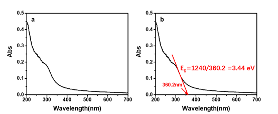
Figure 3 Calculation of bandgap width Eg by cutting method
Method 2, Tauc plot: the above cutting line method is applicable to the direct bandgap of transmission spectrum that limits its large application. Tauc plot is mainly based on the formula proposed by Tauc, Davis and Mott et al.: (αhν)1/n = B(hν-Eg) , where α is absorption coefficient, h is Planck-constant, ν is frequency, B is constant, Eg is the bandgap width of semiconductor, Exponential n is directly related to the type of semiconductor, direct bandgap n=1/2, indirect bandgap n=2。
Based on the above formula, we know that (αhν)1/n is only linear with hν, which can be used to estimate Eg. When calculate Eg by Tauc plot method, either “Abs” or “α” has no effect on Eg value (only the coefficient B is different), for simplicity, the absorbance value “Abs” can be directly used to replace the absorption coefficient “α”.
Taking In2O3 sample as an example, the steps are as follows:
In2O3 is uniformly spin-coated on quartz slice, and other quartz slice is used as the baseline to test the absorption spectrum of the sample:
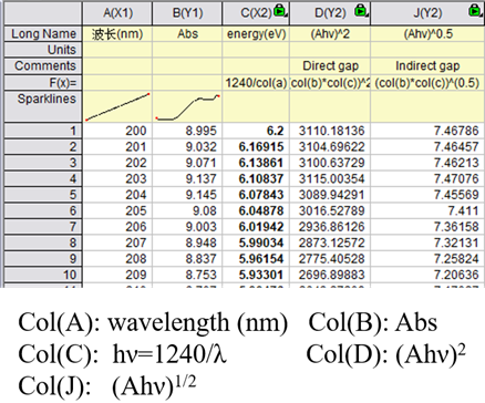
Figure 4 Tauc plot absorption spectrum method for calculation of bandgap
In the origin software, the parameters of each column are designed in Figure 4, because the In2O3 is n-type broadbandgap semiconductor with both the direct bandgap and indirect bandgap. For calculating the direct bandgap, n = 1/2, (Ahν)2= hν-Eg; for calculating indirect bandgap, n = 2, (Ahν)1/2= hν-Eg. As shown in Figure 5, hν sets as x axis, (Ahν)2 and (Ahν)1/2 set as y axis, and reversely extend tangent line intersected with the x axis, The intersection on x axis is the value of optical bandgap. In deail, the direct Eg = 3.68 eV , and the indirect bandgap Eg = 2.85 eV, which were equal to the previously published results that direct bandgap Eg = 3.6 eV[1-2] and indirect bandgap Eg = 2.8 eV[2].

Figure 5 Calculation of direct and indirect bandgap of In2O3
In addition to absorption spectra, UV-VIS-NIR diffuse reflection spectra can also be used for the calculation of direct and indirect bandgap according to the Kubelka-Munk formula which derived from the reflection theory established by the two scientists Zeit.fur Tekn. Physik in 1931:
(F(R)hν)1/n =K/S=(1-R)2/2R= B(hν-Eg)
Where the K is absorption coefficient, S is the reflection coefficient, R is reflectivity (%), h is Planck's constant, ν is the frequency of the light, Eg is a physical quantity related to the material, that is, the energy bandgap, n=1/2 for indirect bandgap semiconductor, n=2 for direct bandgap semiconductor. Plot the curve with (F(R)hν)1/n as y axis, and hν as x axis. Fitting the linear section of the curve, the obtained intersection on the x axis is the bandgap energy.
Taking Ga2O3 sample as an example, the steps are as follows:
BaSO4 whiteboard was used as the baseline of reflection spectrum, and then the sample was uniformly spin-coated on BaSO4 base to test the reflectance R of the sample. The detailed data processing as shown in Figure 6.
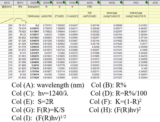
Figure 6 Calculation of bandgap by Tauc plot reflection spectrum
In the origin software, the parameters of each column are designed in Figure 6, because the Ga2O3 is direct bandgap semiconducting, where n = 1/2, Plot curve with the function (F(R)hν)2= hν-Eg. As shown in Figure 7, set hν to the x axis, set (F(R)hν)2 to the y axis, and reversely extend tangent line intersected with the x axis, The intersection on x axis is the value of the optical direct Eg = 4.72 eV , which equals to the previously published results that Eg=4.5~4.9 eV[3-4].
If the sample is an indirect bandgap semiconductor, just replace the y axis with (F(R)hν)1/2 to plot, reverse extension curve tangent to intersect with the x axis, you can get the optical indirect bandgap value of semiconductor materials.
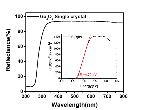
Figure 7 Direct bandgap calculation of Ga2O3
In this topic, we systemically introduce how to measure the bandgap width of semiconductor by UV-VIS-NIR spectrophotometer. Welcome to ISCMS Spectroscopy Lab to discuss and perform experiments on UV-VIS-NIR spectrophotometer.
Reference:
1. Li, C, Zhang, D, Han, S, Liu, X, Tang, T and Zhou, C, Diameter‐Controlled Growth of Single‐Crystalline In2O3 Nanowires and Their Electronic Properties. Adv. Mater, 2003, 15, 143-146.
2. Yutaka Ohhata, Fujitoshi Shinoki, Sadafumi Yoshida, Optical properties of r.f. reactive sputtered tin-doped In2O3 films, Thin Solid Films, 1979, 59, 255-261,
3. Rafique S, Han L, Zhao H. Synthesis of wide bandgap Ga2O3 (Eg∼ 4.6–4.7 eV) thin films on sapphire by low pressure chemical vapor deposition[J]. physica status solidi (a), 2016, 213, 1002-1009.
4. Rafique S, Han L, Zhao H. Ultrawide bandgap β-Ga2O3 thin films: growths, properties and devices[J]. ECS Transactions, 2017, 80, 203.