【光谱实验室:陈中博士 撰文】
【仪器设备:快速成像显微拉曼光谱仪WITec R300】
【地点:4号楼220室 光谱实验室】
【文章来源:Nature Nanotechnology 2020. Huang, M., Bakharev, P.V., Wang, Z. et al. Large-area single-crystal AB-bilayer and ABA-trilayer graphene grown on a Cu/Ni(111) foil. https://doi.org/10.1038/s41565-019-0622-8】
拉曼光谱是一种快速而又简洁的表征二维材料结构的方法。目前研究最多的二维材料之一石墨烯,其sp2碳原子紧密堆积形成的二维原子晶体结构可以通过拉曼G峰、D峰和2D峰的峰位、峰型以及强度进行分析,从而能进一步了解石墨烯的层间堆垛方式、掺杂、温度和应力等对石墨烯的电子能带结构的影响。近日,文章发表在《Nature Nanotechnology》的韩国国立蔚山科学技术院 Rodney S. Ruoff 等人在首次报道一种基于化学气相沉积法(CVD法)在单晶Cu/Ni(111)合金箔表面制备的超大面积且高质量的AB堆叠双层和ABA堆叠三层石墨烯薄膜。通过拉曼光谱和透射电镜对石墨烯薄膜的堆积顺序、覆盖范围和均匀性进行了评估。

图1 Cu/Ni(111)箔的制备与表征。 a. 制备Cu/Ni(111) 箔片的示意图。b. Cu/Ni(111) 箔片照片。c. 整个样品(3×5 cm2)不同区域的XRD图谱。 d. Cu/Ni(111)箔片的EBSD图谱,Scale bar 90 μm。
研究人员首先通过热处理的方法调控Ni元素的浓度,精确控制Ni原子的量与Cu(111)箔片形成单晶Cu/Ni(111)合金箔,并用XRD和EBSD map确定制备的薄膜的结晶度及表面信息(图1)。 研究发现,Ni元素的浓度在10.2%时,碳元素通过化学气相沉积在Cu/Ni(111)合金箔表面只生长出单层石墨烯,增加Ni元素浓度将生长出双层和三层石墨烯薄膜,Ni元素的浓度在16.6%时,得到高质量的双层石墨烯薄膜(> 95%),Ni元素的浓度在20.3%时,得到高质量的三层石墨烯薄膜(> 60%)。随后,研究人员将样品转移至300 nm的SiO2/Si 衬底进行光学成像和拉曼表征。
在图2a中,拉曼光谱上的D峰消失说明此石墨烯是高质量的且基本无缺陷的。根据前人的报道结果,高分辨拉曼光谱中的2D峰与G峰的比值能判断石墨烯的层数,作者对其中的双层和三层薄膜进行了详细分析。图2b中,双层石墨烯图谱上不对称的2D峰通过洛伦兹拟合出4个对称峰表明石墨烯的AB双层方式的堆叠。同样,三层石墨烯图谱上不对称的2D峰通过洛伦兹拟合出6个对称峰表明石墨烯的ABA三层方式的堆叠。光学显微照片(图2c, f, i)上能看出石墨烯从离散的单片生长到大面积的双层、三层薄膜的过程。每个样品都对其ID/IG比值和2D 峰的半峰宽进行拉曼mapping处理。在完全形成双层薄膜后,其ID/IG的比值基本一致(图g),说明此双层薄膜的是高质量和均匀的。特别是对半峰宽进行mapping(图h),研究发现,双层区域所有的半峰宽都是一致的(红色区域),与ID/IG的比值的结果吻合。同时,图像上很容易看出优化后的双层薄膜接近100% AB堆叠双层结构,而且分布非常均匀。同样,对三层石墨烯进行同样的拉曼分析,发现此方法所得的样品具有60%以上的ABA堆叠结构。作者采用TEM和SAED表征手段(TEM和SAED结果参见原文)再次证明了石墨烯的层数和堆叠结构,所得的结论和拉曼分析的结果一致。
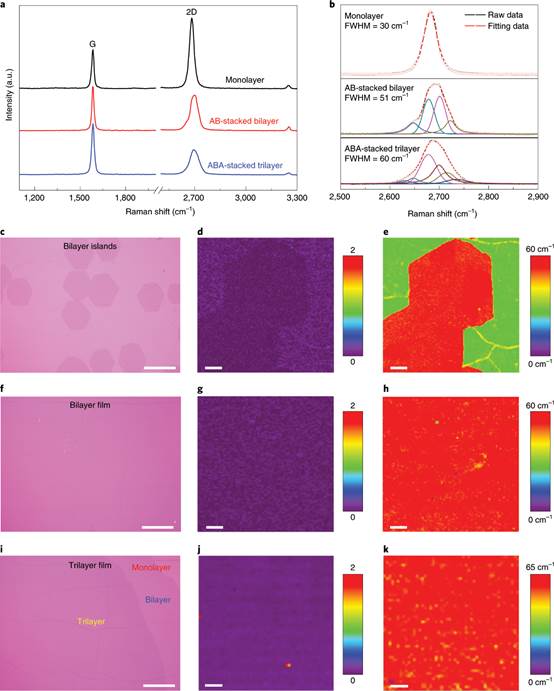
图2 拉曼光谱和拉曼成像表征双层和三层石墨烯。a. 单分子层、双分子层和三层石墨烯的拉曼光谱。b. 单层、双分子层和三层石墨烯薄膜的2D峰的洛伦兹拟合。c-k. 分别为双层片(c-e) 、连续双层膜 (f-h) 和三层膜 (i-k) 的光学图像、ID/IG比值和2D 峰半峰宽的拉曼mapping。Scale bar 50 μm。
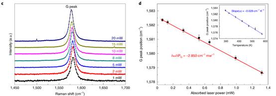
图3 c. 不同激光功率下悬浮双层石墨烯的拉曼光谱, 当激光功率增加时,G峰出现明显的红移。d. 双层石墨烯吸收激光功率与G峰位移的关系及计算出的热导率。
为了进一步探究单晶Cu/Ni(111)合金箔法所制备的双层石墨烯的性能,作者用非接触式拉曼光热技术来研究双层石墨烯的热导率。图3d插图中的变温拉曼光谱(300 K - 600 K)证明了G 峰的位置是与温度是相关的。通过改变激光功率导致G峰峰位的变化,作者计算出此方法生长的AB堆叠双层石墨烯的热导率为~2300 W m-1 K-1,远高于其他CVD法制备的双层石墨烯(657 - 1413 W m-1 K-1),也高于其他方法制备的AB堆叠双层结构(1896 W m-1 K-1),仅次于机械剥离法制备的AB堆叠双层结构(~2800 W m-1 K-1)。优异的热导性能进一步表明了此方法制备的大面积AB堆叠双层石墨烯薄膜具有高质量和均匀性。
文章中采用的拉曼光谱仪与理化平台光谱实验室的WITec R300快速成像拉曼光谱仪(https://iscps.westlake.edu.cn/info/1024/1451.htm)是同型号的,其光谱分辨率高和快速成像的特点使其对结构分析非常高效,所得结论与电镜结果完全一致。文献作者通过非接触式拉曼光热技术还能判断双层石墨烯性能的优劣,此性能测试所需要的条件在理化平台的拉曼仪器上也能完全满足。理化平台所配的温度测试附件在77 K - 873 K可调,功率调节精度低至0.1 mW,远高于其他型号的拉曼光谱仪,欢迎有需要的广大研究人员来预约使用。
参考论文:Huang, M., Bakharev, P.V., Wang, Z. et al. Large-area single-crystal AB-bilayer and ABA-trilayer graphene grown on a Cu/Ni(111) foil. Nat. Nanotechnol. (2020). https://doi.org/10.1038/s41565-019-0622-8
论文链接:https://www.nature.com/articles/s41565-019-0622-8
High resolution Raman spectroscopy and rapid Raman maps used to analyze the structure and performance of large-area single-crystal AB-bilayer and ABA-trilayer graphene
Raman spectroscopy is a fast and simple method to characterize the structure of two-dimensional materials. Graphene is one of the most studied two-dimensional material, whose sp2 carbon atoms tightly packed into a two-dimensional atomic crystal structure can be achieved by analysis of position, shape and intensity of Raman G, D and 2D peak, which can be of help for further understanding that how the stacking of graphene layers, doping, temperature and strain influence on the electronic band structure of graphene. Recently, Rodney S. Ruoff et al, UNIST, Ulsan, Republic of Korea, published a paper in 《Nature Nanotechnology》 that developed an AB-stack bilayer and ABA-stack trilayer graphene film with a super-large area and high quality on the surface of single crystal Cu/Ni(111) alloy foil by chemical vapor deposition. Their stacking sequence, coverage and uniformity of graphene films were evaluated by Raman spectroscopy, Raman maps and transmission electron microscopy, etc. Also, their performance like their thermal conductivity measurement was achieved by non-contact Raman optothermal technique.
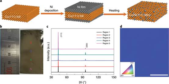
Fig. 1 Preparation and characterization of Cu/Ni(111) foils. a. Schematic of the preparation of the Cu/Ni(111) foils. b. Photograph of an as-prepared Cu/Ni(111) foil. c. XRD patterns taken from different regions across the whole sample (3 × 5 cm2), as indicated in b. d. EBSD map of the Cu/Ni(111) foil. Inset: colour code for the inverse pole figure. Scale bar, 90 μm.
The researchers firstly regulated the concentration of Ni elements by heat treatment, accurately controlled the formation of single crystal Cu/Ni(111) alloy foil by Ni atoms and Cu(111) foil, and used XRD and EBSD map to determine the crystallinity and large area single-crystal Cu/Ni(111) alloy foil of the prepared film (Fig. 1). It was found that when the concentration of Ni element closes to 10.2%, the CVD method used in Cu/Ni(111) alloy foil surface only grow a single-layer graphene. Increasing the concentration of Ni element will continue to grow bilayer and trilayer graphene films. The concentration of Ni element up to 16.6% can achieve high quality AB-bilayer graphene films. When the concentration of Ni element rises up to 20.3%, trilayer graphene films with high quality can be prepared. The samples then transfer to 300 nm of SiO2/Si substrate for optical imaging and Raman characterization.
In Fig. 2a, the absence of D peak on the Raman spectrum demonstrates that the graphene is of high quality and basically defect-free. The ratio of 2D peak to G peak in the high resolution spectrum can determine the number of graphene layers. In Fig. 2b, the asymmetric 2D peaks on the bilayer graphene can be fitted by four Lorentzian peaks, indicating the AB bilayer mode of graphene stacking. Similarly, the 2D band of trilayer graphene was fitted by six Lorentzians (Fig. 2b) and shown to be ABA, as per Raman studies on exfoliated ABA-stacked trilayer graphene flakes and CVD-grown trilayer graphene samples. Optical images (Fig. 2c, f, I) show the growing process of graphene from discrete islands to large-area bilayer film. Raman mapping of ID/IG ratio and 2D FWHM were filtered to investigate the uniformity of samples. After fully formed bilayer film, the ratio of its ID/IG keeps consistent (Fig. 2g). The 2D FWHM mapping (Fig. 2h) result also confirm the uniformity of bilayer graphene. The above two kinds of mapping results are consistent. It's easy to observe from those images that the nearly 100% AB stacked bilayer structures formed and is very uniform. Similarly, ABA stacking of trilayer graphene also grew uniform coverage up to 60%. The number of layers and the stacking order of the graphene samples were also examined by Transmission electron microscopy (TEM) studies and selected area electron diffraction (SAED) measurements, in which the results are the same as Raman analysis. (TEM and SAED see original paper)

Fig. 2 Raman measurements of the bilayer and trilayer graphene. a. Raman spectra of monolayer, AB-stacked bilayer and ABA-stacked trilayer graphene transferred onto SiO2/Si substrates. b. Lorentzian fit of the 2D peaks for monolayer, AB-stacked bilayer and ABA-stacked trilayer graphene films. c–k. Optical images and Raman maps of the ID/IG ratio and 2D FWHM respectively of bilayer islands (c–e), a continuous bilayer film (f–h) and a trilayer graphene film (i–k). Scale bars, 50 μm (c,f,i) and 10 μm (d,e,g,h,j,k).
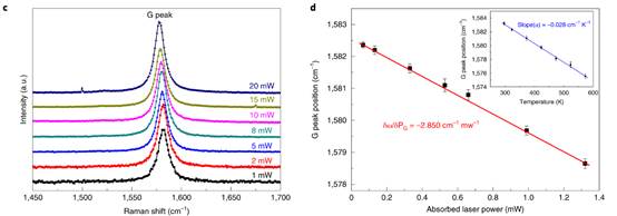
Fig. 3 c. Raman spectra of suspended bilayer graphene obtained at different laser powers. A clear red shift of the G peak was observed when the laser power was increased. d. G peak position shift versus absorbed laser power by bilayer graphene. The inset shows the temperature dependence of the G peak position for bilayer graphene.
In order to further explore the performance of bilayer graphene prepared by this CVD method, their thermal conductivity was studied by non-contact Raman optothermal technique. The variable temperature Raman spectrum (300 k - 600 k) in Fig. 3d inset proves that the position of G peak is temperature dependent. By studying the absorbed laser power related with G peak position shift, the authors calculate the bilayer thermal conductivity of graphene is ~ 2300 W m-1 K-1, far higher than other CVD method of bilayer graphene (657-1413 W m-1 K-1), also higher than other methods of preparation AB stacking bilayer structure (1896 W m-1 K-1), and is more like that of an exfoliated bilayer graphene flake (~ 2800 W m-1 K-1). The excellent thermal conductivity further demonstrates the high quality and uniformity of the AB-stacked bilayer graphene film.
"Fast-Mapping Micro-Raman Spectrometer" (WITec R300) used in this paper is the same as the instrument in our Spectroscopy Lab of ISCPS (https://iscps.westlake.edu.cn/info/1024/1451.htm). Its high spectral resolution and fast mapping make the structure analysis is very effective and efficient, where the structural analysis is consistent with TEM and SAED. In the literature the authors can also measure the performance of graphene by non-contact Raman photothermal technique. In our lab, the temperature-control range of WITec R300 covers from 77 k to 873 k, and the laser power can be adjusted accurately to 0.1 mW. The accuracy is much higher than that of other Raman spectrometers, which can not only complete the similar work in the paper, but also be more perfect and systematic. Welcome to the Spectroscopy Laboratory of ISCPS to inquire and use "Fast-Mapping Micro-Raman Spectrometer".
Reference:Huang, M., Bakharev, P.V., Wang, Z. et al. Large-area single-crystal AB-bilayer and ABA-trilayer graphene grown on a Cu/Ni(111) foil. Nat. Nanotechnol. (2020). https://doi.org/10.1038/s41565-019-0622-8
Link:https://www.nature.com/articles/s41565-019-0622-8